01
The “Heating and Warpage Crisis” of High-Power Chips
With large models such as DeepSeek opening the door to the application of AI technology, the construction of data centers with high-computing power AI chips as the core has ushered in rapid development. The exponential increase in power consumption of AI chips is in significant contradiction with the linear expansion of physical size, which directly leads to a significant increase in power density. Taking H100 as an example, its maximum power consumption can reach 700W, the chip size is 814mm², and the chip warpage problem caused by long-term high-power operation and heating is becoming more and more serious. According to research, for every 10°C increase in chip temperature, its reliability can be reduced by about 50%. Therefore, efficient heat dissipation is essential to maintain the stable and efficient operation of AI chips.

Figure 1 The power consumption of foreign mainstream AI chips is rising (compiled by HFC according to public information)
In the construction of the chip thermal conduction system, we functionalize the different levels of thermal interface materials (TIMs):
TIM1.5: Thermal interface material for direct connection of bare die to heat sink
TIM1: The thermal interface material between the chip and the Lid in a package with Lid
TIM2: The thermal interface material between the Lid and the heat sink in a package with Lid

Fig.2 The use scenario of HFC TIM&TIM2 graphene thermal pad
Take the TIM1 scenario of a high-power and large-size chip as an example:
The thermal interface material needs to meet the requirements of low BLT (≤0.3mm), low thermal resistance (≤0.1°Ccm²/W), and stress absorption (warpage caused by different CTEs in the upper and lower CTEs) at the same time.
Traditional silicone grease, phase change thermal conductive materials, and indium flakes all meet the requirements of low BLT and low thermal resistance, but they still have great difficulties in the face of structural deformation caused by the mismatch of the coefficient of thermal expansion (CTE) of the material. When the system continues to run at high power, the substrate, chip, and heat sink will warp by 0.1-0.3mm due to the difference in CTE. This dynamic deformation will not only reduce the heat conduction efficiency of TIM materials, but also cause the “pump-out phenomenon” of interface materials, which is positively correlated with the package size, and its destructiveness is much greater than that of small-size packages above 1000mm², which directly threatens the reliability and life of the product.
HFC is a leading enterprise in the research and commercialization of thermal interface material orientation process in China. On the basis of the successful experience of developing oriented carbon fiber thermal pads in 2018, the longitudinal graphene thermal pads were successfully developed through the orientation process, which successfully solved the heat dissipation problem of high-power and large-size chips.

Figure 3: HFC longitudinal graphene thermal pad
02
How does HFC longitudinal graphene thermal pad solve the problem of heat dissipation of high-power and large-size chips?
(1) Low BLT problem: Through the ultra-thin process, the maximum compression amount can be used with 70%, and the BLT in the chip packaging TIM scenario can reach 0.1mm.
(2) Low thermal resistance: The theoretical thermal conductivity of single-layer graphene can reach 5300W/mK, and the thermal resistance is as low as 0.04°Ccm²/W after applying a suitable packaging pressure through the orientation process.
(3) Large-scale warpage problem: through the internal porous structure, it can quickly adapt to the local deformation of the interface. Prevent the material from being extruded from the interface, eliminate the formation of interface voids, perfectly absorb warpage displacement, and ensure long-term reliability.
(4) High reliability: Through the rigorous 1000h high temperature, high and low temperature impact and double 85 aging tests of HFC’s internal CNAS accredited laboratory and mass production customer laboratory, the thermal resistance change rate of graphene thermal pads is <5%, and the reliability is significantly better than that of conventional thermal interface materials.
(5) High-quality mass commercialization: HFC longitudinal graphene thermal pad has accumulated many years of experience in chip heat dissipation application, has realized automated production line and mass production delivery, and its product quality has been recognized by many leading enterprises in the chip industry at home and abroad and won the “Quality Excellent Collaboration Award”.
(6) Leading in independent innovation: HFC is a manufacturer of innovative EMC and thermal interface materials, longitudinal graphene gasket has original process equipment and technical patents, and has a complete series of industrial intellectual property rights. Production bases have been laid out in Shenzhen, Malaysia, Thailand and other places to meet the supply needs at home and abroad.

Fig.4 HFC graphene thermal pad is composed of longitudinal continuous, high thermal conductivity and low-density graphene

Fig.5 The application scenario of HFC graphene thermal pad, the thermal resistance is as low as 0.04°Ccm²/W
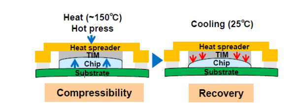
Fig.6 HFC graphene thermal pad with high resilience can absorb warpage deformation of substrates, chips and heat sinks
03
In the chip packaging TIM1/TIM1.5 scenario, HFC graphene thermal pad adopts the performance and production process advantages of HFC graphene thermal pad compared with traditional thermal interface materials such as thermal grease and indium sheet
Compared with traditional thermal grease materials, graphene thermal pads have no risk of creep and pump-out, and the high elastic fit can cope with the warpage of large-size chips, and the thermal interface is regular and complete, and the heat conduction is uniform without hot spots. It will not dry out after long-term high-temperature operation, and the thermal resistance is more stable for long-term aging. The siloxane content is very low, which can meet the application scenarios of chip heat dissipation with low volatile requirements.
Compared with indium sheets for packaging, graphene thermal pads have a simple process and can be automatically placed without complicated processes, which greatly saves packaging time and equipment investment costs. The existing packaging process of indium wafer requires gold plating on the chip/LID, and flux spray and vacuum reflow soldering are required for placement, which is prone to problems such as large void, melt reflow pollution, and containment failure.
Typical application scenarios of graphene thermal pads
